Charge-coupled device (CCD) and charge storage device (Memory), as two independent branches in modern electronic systems, have developed along their respective paths. Prototype devices with photoelectric sensing and storage functions have not been reported yet. Recently, researchers from the Shenyang National Research Center for Materials Science, Institute of Metal Research, Chinese Academy of Sciences have cooperated with many domestic units to publish an online titled "Flexible Carbon Nanotube Sensing-Storage Device" in Advanced Materials nanotube sen-memory device).
Researchers have proposed a carbon nanotube non-volatile memory based on an aluminum nanocrystal floating gate, with a high current switching ratio, a storage time of up to 10 years, and stable read and write operations, multiple discrete aluminum nanocrystals Floating gate devices have stable flexible performance. More importantly, the tunneling mechanism of the charge in the AlOx layer generated by oxidation changes from Fowler-Nordheim tunneling to direct tunneling, thereby realizing the sensing and detection of photoelectric signals; based on theoretical calculation analysis and experimental optimization Designed and prepared a 32 × 32 pixel non-volatile flexible ultraviolet array device. It realized the sensing and image storage of optical images for the first time, which laid the foundation for the development of new flexible light detection and storage devices.
Researchers use semiconducting carbon nanotube film as the channel material, and use a uniformly distributed aluminum nanocrystal / alumina integrated structure as the floating gate layer and tunneling layer to obtain high-performance flexible carbon nanotube floating gate memory (Figure 1 ) To achieve a current switching ratio between read and write and erase of the device at a bending strain of 0.4% higher than 105 and storage stability exceeding 108s (Figure 2). At the same time, the thinner aluminum oxide tunneling layer allows the carriers "trapped" in the aluminum nanocrystal floating gate in the erased state to return to the channel by direct tunneling when obtaining light energy higher than the aluminum work function Among them, the closed-state current is significantly improved, the direct conversion and transmission of photoelectric signals are completed, and a new multi-functional photoelectric sensor and storage system that combines image sensing and information storage is realized (Figure 3).
The research work was proposed by Sun Dongming and Qu Tingyu of the Institute of Metals, and was completed in collaboration with Qiu Song and Li Qingwen, researchers at the Suzhou Institute of Nanotechnology and Nanobionics, Chinese Academy of Sciences, Professor Wang Wei from Jilin University, and researchers from the Institute of Metals. Qu Tingyu and Sun Yu carried out device preparation, electrical measurement and data analysis, Chen Maolin conducted device technology research such as electron beam exposure, Qiu Song and Li Qingwen synthesized semiconductor carbon nanotube solutions, and Liu Zhibo conducted transmission electron microscopy of the samples Characterization, Tan Jun carried out sample processing such as focused ion beam. All authors participated in the data analysis discussion and thesis writing. Qu Tingyu, Sun Yu, and Chen Maolin are co-first authors, and Qiu Song, Han Zheng, Cheng Huiming, and Sun Dongming are co-corresponding authors. The research work was supported by the National Natural Science Foundation of China, Chinese Academy of Sciences, Institute of Metals, Shenyang National Research Center for Materials Science, Youth Thousand Talents Program, and National Key R & D Program.
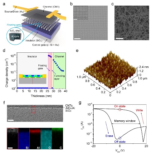
Figure 1. Device design and structure.
a) Schematic diagram of device structure; b) Aluminum / alumina nanocrystal lattice structure with uniform and discrete distribution and c) SEM image of carbon nanotube film channel material; d) Simulation of charge density distribution in the channel; e) Aluminum nanocrystal surface Topography; f) Cross-sectional TEM and element distribution of carbon nanotube film and floating gate layer structure; g) Storage window.
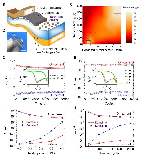
Figure 2. Flexible device electrical performance and flexibility characterization.
a) Schematic diagram of flexible device structure and b) physical picture; c) optimization of conditions of aluminum nanocrystal / alumina integrated structure; d) device retention characteristics and e) cycle performance characterization; device f) different bending stress and g) times Flexible characterization.
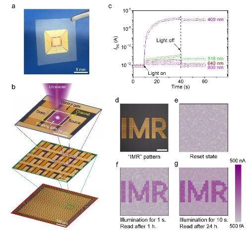
Figure 3. Device photoelectric response and image storage.
a) Flexible sensing storage device; b) Device structural unit; c) Optical response characteristics at different wavelengths; dg) Characterization of device optical storage characteristics.
Dosing Equipment,Ingredient Dosing Equipment,Chemical Dosing Equipment,Liquid Dosing Equipment
Zhejiang Ailipu Technology Co., Ltd. , https://www.alipu.com