Single-walled carbon nanotubes have excellent mechanical, electrical and optical properties, and can be used as transparent electrode materials or semiconductor channel materials in the field of flexible and transparent electronic devices, so they are considered to be one of the most competitive candidate materials. The development of a method for efficiently and macroscopically preparing high-quality carbon nanotube films has become a key challenge for the practical application of this material. First of all, the size of single-walled carbon nanotube films prepared so far is usually in the order of centimeters, and the batch preparation method cannot meet the requirements for large-scale applications. Secondly, impurities and structural defects are usually introduced during the preparation process of the carbon nanotube film, which deteriorates the photoelectric performance of the film, which is far lower than the theoretically predicted value. Therefore, it is of great value to develop a method for preparing high-quality single-walled carbon nanotube thin films with high efficiency and high volume.
Recently, the team of Sun Dongming and the team of Liu Chang of the Advanced Carbon Materials Research Department of the Institute of Metal Research, Chinese Academy of Sciences have proposed a technology for the continuous synthesis, deposition and transfer of single-walled carbon nanotube thin films, which achieves high-quality single-walled carbon nanometer-scale nanometer Continuous preparation of tube thin films, and based on this, high-performance all-carbon thin film transistor (TFT) and integrated circuit (IC) devices are constructed. The researchers used a floating catalyst chemical vapor deposition method to continuously grow single-walled carbon nanotubes in the high-temperature region of the reactor, and then collected the prepared carbon nanotubes at room temperature through a gas-phase filtration and transfer system, and transferred them by roll-to-roll transfer. On the flexible PET substrate, a single-walled carbon nanotube film with a length of more than 2m was obtained. A fluid simulation of the filtration and deposition process showed that when the air outlet speed was adjusted so that the suction filtration process was in equilibrium, the airflow in the filtration system showed a uniform airflow velocity distribution (Figure 1). The single-walled carbon nanotube film prepared by this method exhibits excellent photoelectric performance and uniformity of distribution. At a wavelength of 550 nanometers, the light transmittance is 90%, and the sheet resistance is 65Ω / □ (Figure 2). The researchers used the prepared carbon nanotube film to construct high-performance all-carbon flexible transparent transistors (Figure 3) and XOR gates, 101-order ring oscillators and other flexible all-carbon integrated circuits (Figure 4).
This is the first time that researchers have developed a continuous growth, deposition and transfer technology of single-walled carbon nanotube films with a length in the order of meters. The prepared single-walled carbon nanotube films and their transistors have excellent photoelectric properties, and are based on single-wall The large-area, flexible and transparent electronic devices of carbon nanotube films lay the foundation for materials. This work was supported by the National Natural Science Foundation of China, the National Key R & D Program, the China Postdoctoral Science Fund, the Equipment Development Program of the Chinese Academy of Sciences, the Liaoning Ten Million Talent Program, and the Youth Thousand Talents Program. The continuous preparation technology of single-walled carbon nanotube film has obtained the Chinese invention patent (ZL201410486883.1), and related papers were published online in Advanced Materials recently.
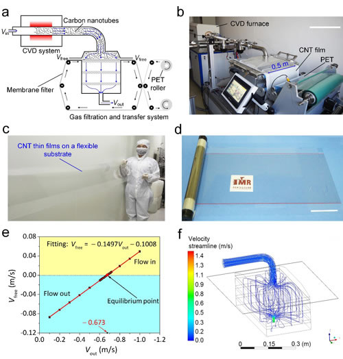
Figure 1 Preparation of meter-scale single-walled carbon nanotube film. (A) Schematic diagram of the continuous synthesis, deposition and transfer process of carbon nanotubes. (B) Diagram of experimental device. (C) Single-walled carbon nanotube film on flexible PET substrate. (D) A roll of single-walled carbon nanotube film. (E) Simulation curve of gas velocity. (F) Simulation results of airflow distribution in equilibrium.

Figure 2 Characterization of the photoelectric properties of single-walled carbon nanotube films. (A) Characterization of surface distribution of light transmittance. (B) Characterization of square resistance surface distribution. (C) Comparison of film properties.
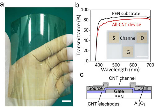
Figure 3 Large area flexible all-carbon device. (A) Photograph of flexible transparent all-carbon device. (B) Device optical transmittance curve. (C) Schematic diagram of all-carbon TFT structure.

Figure 4 All-carbon logic gate and ring oscillator. (A) XOR gate. (B) Optical photo of XOR gate. (C) XOR gate input and output characteristic curve. (D) Optical photo of 101th order ring oscillator. (E) 101-order ring oscillator input and output curves.
Silicate can be used in many industries, it include different kinds of silicate, such as: Potassium Silicate, Potassium Sodium Silicate , Sodium Silicate and so on. Potassium silicate & Potassium sodium silicate with glassy lump and liquid mainly are used for welding industry, also can be used for Agriculture, oil drilling field. Powdery Instant Potassium Silicate is white powdery substance, can fast dissolve in water, resistant to cold and good uniformity. It is a special foamed alkali convenient to be used, transported and stored. Molecular formula: K2O·nSiO2·H2O, n varies with the specification the uses. Powdery Instant Potassium Silicate has better solubility and higher adhension compared with powdery instant sodium silcate and is widely used as adhesive in fireproof material, as auxiliary in drilling liquid of oil field and other special fields.
Silicate
Potassium Silicate,Potassium Silicate Sodium,Potassium Water Glass,Sodium Silicate
SJZ Chenghui chemical co ltd , https://www.chenghuichemicals.com